
Author Affiliations
Abstract
1 National University of Singapore, Department of Electrical and Computer Engineering, Singapore
2 A*STAR (Agency for Science, Technology and Research), Institute of Microelectronics, Singapore
3 Huazhong University of Science and Technology, School of Optical and Electronic Information, Wuhan National Laboratory for Optoelectronics, Wuhan, China
4 Nanyang Technological University, Quantum Science and Engineering Centre, Singapore
Lithium niobate (LN) has experienced significant developments during past decades due to its versatile properties, especially its large electro-optic (EO) coefficient. For example, bulk LN-based modulators with high speeds and a superior linearity are widely used in typical fiber-optic communication systems. However, with ever-increasing demands for signal transmission capacity, the high power and large size of bulk LN-based devices pose great challenges, especially when one of its counterparts, integrated silicon photonics, has experienced dramatic developments in recent decades. Not long ago, high-quality thin-film LN on insulator (LNOI) became commercially available, which has paved the way for integrated LN photonics and opened a hot research area of LN photonics devices. LNOI allows a large refractive index contrast, thus light can be confined within a more compact structure. Together with other properties of LN, such as nonlinear/acousto-optic/pyroelectric effects, various kinds of high-performance integrated LN devices can be demonstrated. A comprehensive summary of advances in LN photonics is provided. As LN photonics has experienced several decades of development, our review includes some of the typical bulk LN devices as well as recently developed thin film LN devices. In this way, readers may be inspired by a complete picture of the evolution of this technology. We first introduce the basic material properties of LN and several key processing technologies for fabricating photonics devices. After that, various kinds of functional devices based on different effects are summarized. Finally, we give a short summary and perspective of LN photonics. We hope this review can give readers more insight into recent advances in LN photonics and contribute to the further development of LN related research.
lithium niobate etching photonics integrated optics nanotechnology devices Advanced Photonics
2022, 4(3): 034003

Author Affiliations
Abstract
Institute of Microelectronics, A*STAR (Agency for Science, Technology and Research), Singapore 138634, Singapore
Gas sensors have a wide variety of applications. Among various existing gas sensing technologies, optical gas sensors have outstanding advantages. The development of the Internet of Things and consumer electronics has put stringent requirements on miniaturized gas sensing technology. Here, we demonstrate a chip-scale silicon substrate-integrated hollow waveguide (Si-iHWG) to serve as an optical channel and gas cell in an optical gas sensor. It is fabricated through silicon wafer etching and wafer bonding. The Si-iHWG chip is further assembled with an off-chip light source and detector to build a fully functional compact nondispersive infrared (NDIR) sensor. The chip size is , and the dimension of the sensor excluding the microcontroller board is . This chip solution with compactness, versatility, robustness, and low cost provides a cost-effective platform for miniaturized optical sensing applications ranging from air quality monitoring to consumer electronics.
Photonics Research
2022, 10(1): 01000261
Author Affiliations
Abstract
1 Institute of Microelectronics, A*STAR (Agency for Science, Technology and Research), Singapore 138634, Singapore
2 Current Address: School of Microelectronics Science and Technology, Sun Yat-sen University, Zhuhai 519082, China
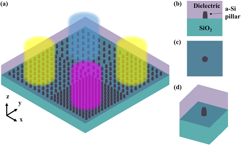
Optical color filters are widely applied in many areas including display, imaging, sensing, holography, energy harvest, and measurement. Traditional dye-based color filters have drawbacks such as environmental hazards and instability under high temperature and ultraviolet radiation. With advances in nanotechnology, structural color filters, which are based on the interaction of light with designed nanostructures, are able to overcome the drawbacks. Also, it is possible to fabricate structural color filters using standard complementary metal-oxide-semiconductor (CMOS) fabrication facilities with low cost and high volume. In this work, metasurface-based subtractive color filters (SCFs) are demonstrated on 12-inch (300-mm) glass wafers using a CMOS-compatible fabrication process. In order to make the transmissive-type SCF on a transparent glass wafer, an in-house developed layer transfer process is used to solve the glass wafer handling issue in fabrication tools. Three different heights of embedded silicon nanopillars (110, 170, and 230 nm) are found to support magnetic dipole resonances. With pillar height and pitch variation, SCFs with different displayed colors are achieved. Based on the resonance wavelength, the displayed color of the metasurface is verified within the red-yellow-blue color wheel. The simulation and measurement results are compared and discussed. The work provides an alternative design for high efficiency color filters on a CMOS-compatible platform, and paves the way towards mass-producible large-area metasurfaces.
Photonics Research
2021, 9(1): 01000013
Author Affiliations
Abstract
1 School of Instrumentation and Optoelectronic Engineering, Beihang University, Beijing 100083, China
2 Singapore Bioimaging Consortium, Agency for Science, Technology, and Research (A*STAR), Singapore 138667, Singapore
3 Institute of Microelectronics, Agency for Science, Technology, and Research (A*STAR), Singapore 138634, Singapore
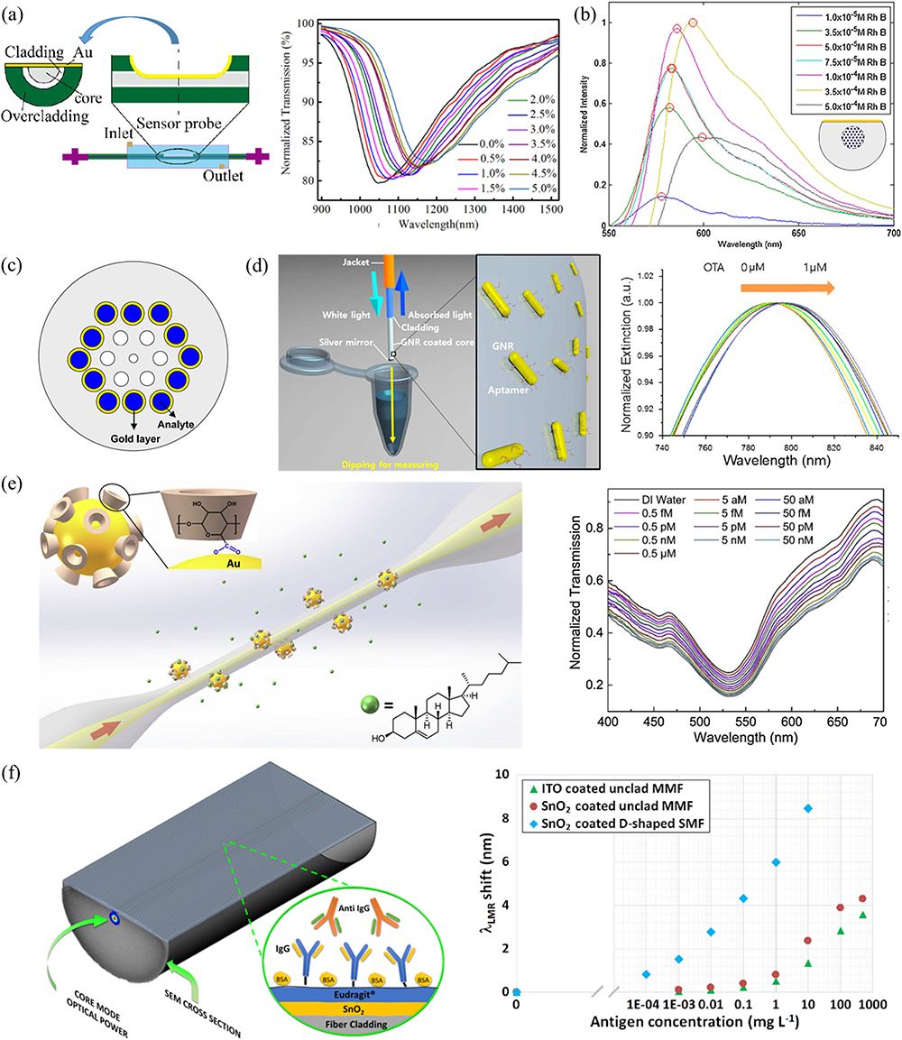
The flexibile nature of optical fiber enables it to offer remote-access capabilities, which could be used in many biomedical applications. This review focuses on different micro- and nano-structured fiber probes for applications in biosensing, imaging, and stimulations. The modifications to fiber could extend design freedom from waveguide optimization to functional material integration. Fiber probes with optimized waveguide structures or integrated functional materials could achieve enhanced optical mode interaction with biosamples, and hence obtain ultrasensitive biosensors with a remarkably low limit of detection. Furthermore, bioimaging with a high spatial resolution can be obtained by engineering dispersion and nonlinearity of light propagation in the fiber core or designing a metal-coated tapered fiber tip with a sub-wavelength aperture. Flat metasurfaces can be assembled on a fiber tip to achieve a large depth of focus and remove aberrations. Fiber is also a compact solution to realize the precise delivery of light for in vivo applications, such as deep brain stimulation. The optical beam size, shape, and direction could be steered by the probe parameters. Micro- and nano-technologies integrated with fiber contribute to various approaches to further improve detection limit, sensitivity, optical resolution, imaging depth, and stimulation precision.
Photonics Research
2020, 8(11): 11001703


